


Executive Summary
GlobalFoundries said on October 8 that it will manufacture silicon interposers for TSMC advanced packaging at its Malta, New York, facility under a five-year agreement worth about $2 billion. The interposer is the silicon layer that carries the memory bus between a GPU die and the HBM stacks beside it. Adding capacity there addresses the part of the AI supply chain that has limited accelerator shipments, not the logic fab. GlobalFoundries calls Malta the first US source of silicon interposers for advanced packaging, with volume production expected to ramp in the first half of 2028.
The deal is a supply contract, not a product. GlobalFoundries provides manufacturing service to TSMC and does not take over the packaging line. The signal is that the packaging step, long the quiet gate on AI hardware, is being regionalized. Nearly every accelerator design depends on a comparable interposer step, so a second source on US soil changes lead times and concentration risk more than it changes performance. It does not relieve the current constraint, because the added capacity does not arrive until 2028.
An AI accelerator looks like one big chip. It is not. The compute die is one part. The high-bandwidth memory that feeds it is another. The thing that connects the two at speed is a third, and that third part is a slab of silicon called an interposer.
The wire between memory and compute is the hard part
High-bandwidth memory does not sit on the compute die. It sits beside it, in stacks, because that is where the capacity and the cooling fit. To move data between them fast you need a very wide, very short bus. The interposer provides it. It is a piece of silicon patterned with thousands of microscopic wires that carry the memory bus, and the dies and the memory stacks are mounted on top of it. The whole assembly then rests on an organic substrate that handles power and slower signals to the board.
TSMC builds this stack under the name CoWoS, for chip-on-wafer-on-substrate. For several years the constraint on how many high-end accelerators the industry can ship has not been the leading-edge logic fab. It has been the advanced packaging line, where dies and memory are joined onto the interposer. When NVIDIA and AMD talk about sold-out capacity, the packaging step is usually in the sentence. The same step sits inside a system like GB200 NVL72, where dozens of dies and memory stacks are wired together into one rack.
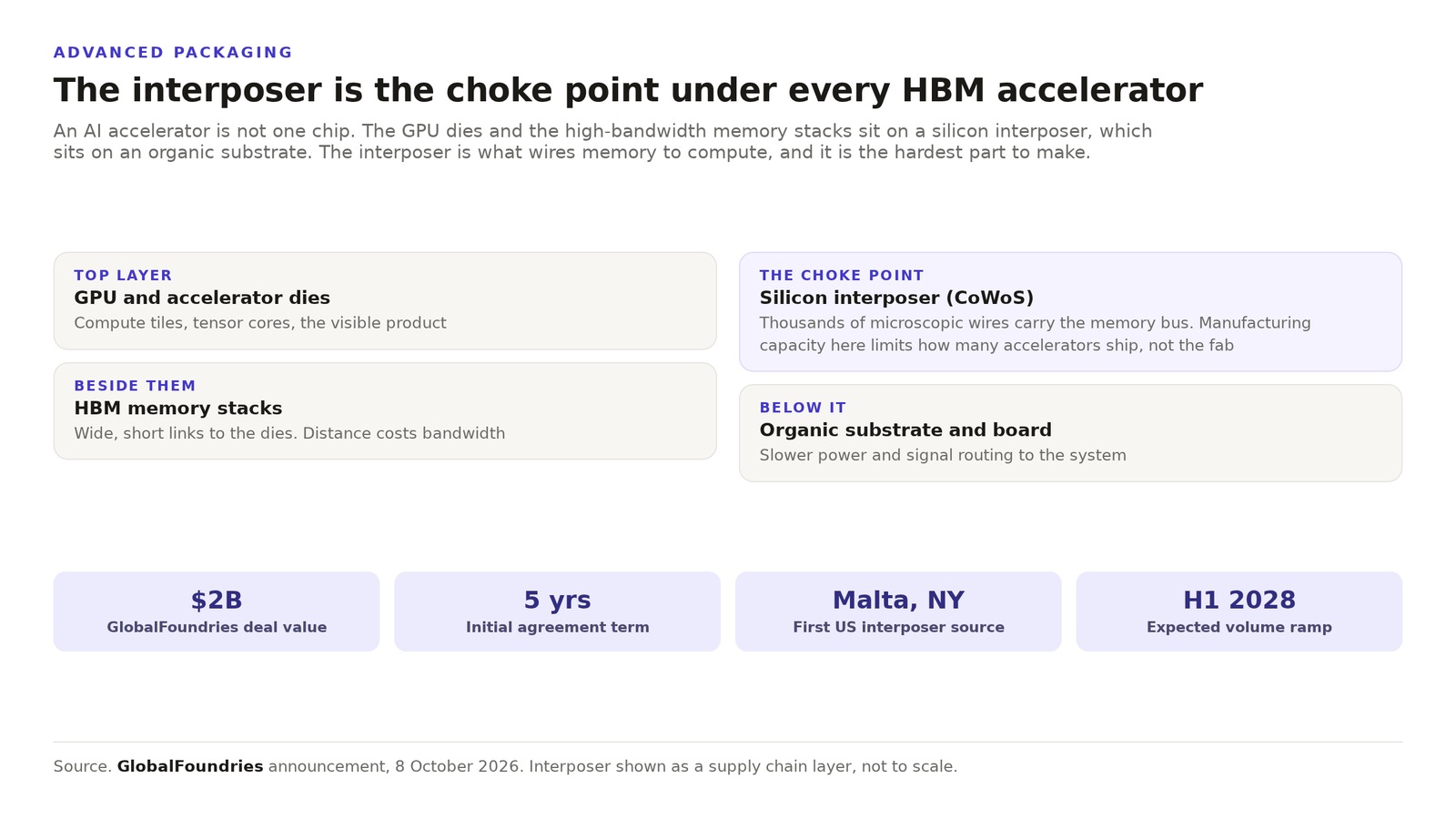
GlobalFoundries is buying into the packaging step, not the fab
Under the agreement, GlobalFoundries will add fabrication capacity at its Malta site to produce silicon interposers for TSMC, which continues to run the wider CoWoS process. GlobalFoundries frames the deal as the first US-based source of silicon interposers for advanced packaging. The initial term is five years, with a framework to expand capacity as demand grows, and the added lines will include embedded deep trench capacitor components. Volume production is expected to ramp in the first half of 2028, according to the announcement.
The value is about $2 billion. That is small next to the tens of billions the same companies spend on leading-edge fabs, which tells you where the perceived risk sits. Interposers are not the scarce logic. They are the scarce connective tissue, and a US source for them is a hedge against a single geography for a part that every accelerator needs. Reuters reported the $2 billion figure and the five-year term.
A US source matters more than another logic lab
For years the advanced packaging step has been concentrated in Taiwan. That concentration is the risk that drives most of the policy talk about sovereign AI, and it is harder to fix than a fab, because packaging is a physical process with its own equipment and its own yield learning. A second source on US soil spreads the risk. It also shortens the loop for US-based accelerator programs that want interposer capacity closer to home.
The honest caveat is that none of this arrives soon. The capacity ramps in 2028, and the interposer constraint is biting now. A five-year, $2 billion contract is a foundation, not a fix. Read it as an admission that packaging, not compute, is the gate, and as the first step in moving that gate.
Ask three questions of your own hardware plan. Which of your accelerator programs depends on a single packaging source? What lead time does your supplier quote for interposer capacity, and how does it compare with the logic die? And if packaging tightens again, which workloads can wait for 2028 capacity and which need to run on hardware you can already buy?
Related reading. Our October 5 piece on NVIDIA rack-scale pricing explains why the unit of purchase moved from the GPU to the whole rack, and why the parts between the chips now set the price.
Get the next one before it is old news
Independent analysis of cloud-native infrastructure, Kubernetes and data center economics. No vendor spin.
[…] Read the full analysis of the interposer bottleneck […]
[…] reading. GlobalFoundries just took the AI chip bottleneck to New York, and the cheapest new AI capacity is the hardware already paid […]